IBM researchers have built the world’s most advanced fully functional integrated circuit made of wafer-scale graphene – a novel semiconductor material that has the potential to improve today’s wireless devices for cheaper, high-speed communications.
The nanotechnology milestone opens up new carbon-based electronics device and circuit applications beyond what is possible with today’s silicon chips.
> See also: Making graphene work
The unique electrical properties of graphene have spurred a tremendous world-wide research effort to take advantage of this new material that is particularly suited for wireless, or radio-frequency (RF), communications.
With the growth of big data applications, higher performance mobile devices become more important to transmit and receive ever increasing data sets more efficiently.
Graphene-based circuits could allow mobile devices such as smart phones, tablets or wearable electronics to transmit much faster data loads to each other and to their surroundings, in a more cost effective and power efficient manner compared to traditional technology solutions.
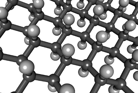
Graphene is one of the thinnest electronic nanomaterials and consists of a single layer of carbon atoms packed in a honeycomb structure. It possesses outstanding electrical, optical, mechanical and thermal properties that make it potentially less expensive and more energy efficient in device applications.
Integration of graphene RF devices into today’s low-cost silicon technology could be a way to enable pervasive wireless communications allowing such things as smart sensors and RFID tags to send data signals at significant distances.
Fabrication of a true integrated circuit is challenging because the atomic dimensions of a sheet of graphene can be easily damaged during the fabrication flow of conventional integrated circuits. A leader in graphene science and technology research, IBM demonstrated a “proof-of-concept” in 2011 showing the world that it was possible to build an analog graphene integrated circuit with a broadband frequency mixer.
> See also: Graphene-based optical switches promise lightning-fast networks
However, the graphene transistor performance was inevitably degraded due to the harsh fabrication processes. Since then, IBM scientists have focused on improving device performance suitable for modern wireless communications.
Using a new approach that leverages mainstream silicon CMOS manufacturing processes, a team of IBM researchers have solved this issue and fabricated and tested the world’s first multi-stage graphene RF receiver, the most sophisticated graphene integrated circuit to date.
To demonstrate true functionality, the researchers were able to transmit a text message – such as you would send and receive on your smart phone – using the graphene integrated circuit, displaying the letters “I-B-M”.
The demonstrated performance is 10,000 times better than previously reported efforts for graphene integrated circuits and is a major leap forward in the realization of a true graphene technology, which will potentially provide higher performance and lower cost wireless communication systems.
'This is the first time that someone has shown graphene devices and circuits to perform modern wireless communication functions comparable to silicon technology,' said Supratik Guha, Director of Physical Sciences, IBM Research.
The breakthrough is also a major milestone for the Graphene Open Manufacturing program, funded by DARPA*, and reported in a paper published today in the journal, Nature Communications.
How it works
The novel approach developed by IBM researchers completely reverses the conventional silicon integrated circuit fabrication flow, leaving graphene transistors as the last step of integrated circuit fabrication, which preserves graphene device performance.
The multi-stage graphene RF receiver integrated circuit consists of 3 graphene transistors, 4 inductors, 2 capacitors, and 2 resistors.
All circuit components are fully integrated into a 0.6 mm2 area and fabricated in a 200 mm (or 8 inch) silicon production line, showing the unprecedented graphene circuit complexity and highest silicon CMOS process compatibility. The new approach also enables the possible heterogeneous 3D integration with a silicon CMOS backbone.
Receivers are one of the key components in any wireless communication systems. The circuits, consuming less than 20 mW power to operate, also demonstrated the highest conversion gain of any graphene RF circuits at multiple GHz frequency.
They successfully received and restored digital text (“I-B-M”) carried on a 4.3 GHz signal without any distortion, showing the feasibility of using graphene integrated circuits in today’s GHz wireless communications.
The scientific paper titled 'Graphene Radio Frequency Receiver Integrated Circuit', by Shu-Jen Han, Alberto Valdes Garcia, Satoshi Oida, Keith A. Jenkins and Wilfried Haensch, appears in Nature Communications.


